- On sale!
Reference: DWM14042301
Spring antenna is specialized for wireless data transmission. This antenna with good performance of V.S.W.R, small size design, easily installation, stable performance and good anti-shock and anti-aged compatible for Hoperf Modules.
Reference: DWM14032902
SMA rf antenna connector is pallets copper gold andexternal thread needle sma pallets plate rf connector.
Reference: DWM14032102
Whip antenna for sub-1 GHz, 433MHz,868MHz and 915MHz with SMA male connectors.it's used with wireless module recommanded by Hoperf .
Reference: DWM14042401
SMA RG178 extension female cable for GPS, GSM antenna,RF module, SMA cable,IPEX to SMA jumper cable.
Reference: DWM18032302
USD3.0/pcs MOQ100pcs LoRa Antenna designed for Lora application which required for outdoor waterproof highgain and work at ISM free band like 433MHz /868MHz /915MHz SMA Male Whip antenna.
Reference: DWM16121503
DWM-TLB-3.0QB SUB-1GHz / 2.4GHz Whip antenna with a Collapsible SMA male connectors.Which are available for 433MHz,868MHz.915MHz and 2.4GHz..
Reference: DWM15101001
Brand: Semtech
RFM50 module series’ design is based on the high performance RF50 SoC chip, It include a CIP-51 core‘ MCU and 100mW transceiver. It operate at 433/470/868/915 MHz ISM band, comply with FCC, ETSI regulation.
Reference: DWM15010504
Brand: Semtech
The RFM69CW /RFM69HCW are built in by SX1231and SX1231H which is ISM Free band transceiver module capable of operation over a wide frequency range, including the 433MHz,868MHz and 915MHz.

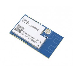
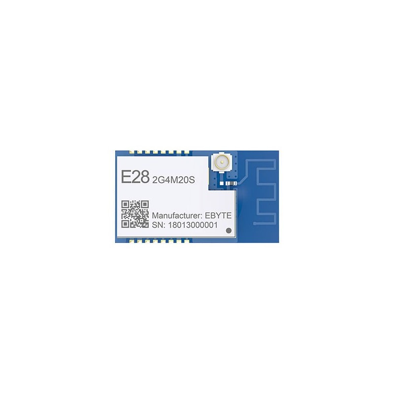
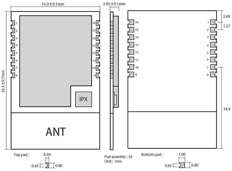
The E28-2G4M20S 2.4GHz SPI +20dBm Enhanced Power LoRa Transceiver Module is based on original imported RFIC SX1280 from SEMTECH, adopts LoRa and FLRC And GFSK Modulation.
The E28-2G4M20S is a 2.4GHz bluetooth module designed by Chengdu Ebyte.The IC SX1280 features multiple physical layers and various modulating methods such as LoRa, FLRC and GFSK. The special modulating and processing methods enable longer operating range with LoRa and FLRC modulating, and the GFSK method covers BLE protocol.
| RF Parameter | Value |
Remark |
| Working frequency |
2400~2500 MHz |
Default: 2.4GHz (52MHz oscillator) |
| Transmitting power | 20 dBm |
About 100mW |
| Receiving sensitivity | -132 dBm |
Air data rate: 125kbps |
| Air data rate | 0.125M~2Mbps |
Default: 125kbps |
| Test distance | 6000m |
In open and clear air, with maximum power, 5dBi antenna gain, height of 2m, air data rate: 125kbps |
| Hardware Parameter | Value |
Remark |
| Size |
26.5 * 15 mm | |
| Antenna type | IPEX / PCB | |
| Communication interface | SPI |
|
| Package | SMD |
|
| Electronic parameter | Min. | Typ. | Max. | Unit | Condition |
| Power supply |
1.8 | 3.3 | 3.6 | V | |
| Communication level | 1.8 | 3.3 | 3.6 | V | |
| Transmitting current |
130 |
140 | 150 | mA | 20dBm(100mW) |
| Receiving current | 9 |
10 | 11 | mA | |
| Sleep current | 1 | 2 | 3 | μA | |
| Operating temperature | -40 | 20 |
+85 | ℃ | |
| Operating humidity | 10 | 60 |
90 | % | |
| Storage temperature | -40 | 20 |
+125 | ℃ |
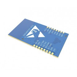
| Pin No. |
Pin Item | Pin Direction | Pin Application |
| 1 | VCC | - |
Power supply, 1.8V ~3.6V (recommend to add external ceramic filter capacitor) |
| 2 | GND | - |
Ground, connecting to power source reference ground |
| 3 | MISO_TX | Output |
SPI data output pin,can be used as UART transmitting pin |
| 4 | MOSI_RX | Input |
SPI data input pin,can be used as UART receiving pin |
| 5 | SCK_RTSN | Input |
SPI clock input pin,can be used as UART request transmitting pin |
| 6 | NSS_CTS | Input |
Module chip selection pin, used to start a SPI communication; and can be used as UART clearing transmitting pin |
| 7 | GND | - |
Ground, connecting to power source reference ground |
| 8 | RX_EN | Input |
LNA controlling pin. Valid under high level |
| 9 | TX_EN | Input |
PA controlling pin. Valid under high level |
| 10 | GND | - |
Ground, connecting to power source reference ground |
| 11 | NRESET | Input |
Chip reset initiation input pin, valid under low level, built-in 50k pull-up resistor |
| 12 | BUSY | Output |
Status indication (refer to SX1280 Datasheet) |
| 13 | DIO1 | Input/Output |
Configurable general IO interface (refer to SX1280 Datasheet) |
| 14 | DIO2 | Input/Output |
Configurable general IO interface (refer to SX1280 Datasheet) |
| 15 | DIO3 | Input/Output |
Configurable general IO interface (refer to SX1280 Datasheet) |
| 16 | GND | - |
Ground, connecting to power source reference ground |
n No
Reference: DWM14073001
Brand: Semtech
APC340 LoRa series rf module is built in RFIC sx1278 and sx1276 which can work on 433MHz,470MHz ,868MHz,915MHz 20dBm Ultra Long Range Transceiver Module with LoRa spread spectrum modulation.
Reference: DWM15123001
Brand: Semtech
HM-TRLR-S series are operating at 433MHz, 868MHz, 915MHz low cost, high performance transparent transceiver with LoRa/FSK/ GFSK/OOK modulation variety.It's mainly use for uav controller and drone data link.
Reference: DWM16092701
RFM98PW / RFM95PW which are Enhanced Power Long Range Transceiver Module.the available versions is RFM98PW 433MHz, and 868MHz,915MHz for RFM95PW.
Reference: DWM16112801
DWM-LoRa1276F30 is a 500W high power wireless transceiver module, which integrates SemtechRF transceiver chip SX1276. There are 868MHz and 915MHz for avaialble options.
Reference: DWM16112802
DWM-LoRa1278F30 is a 500W high power wireless transceiver module, which integrates SemtechRF transceiver chip SX1278. There are 433MHz and 470MHz for avaialble options.
Reference: DWM20030701
Brand: Semtech
The E22-M30S 433MHz /868MHz /915MHz SPI +30dBm Enhanced Power LoRa Transceiver Module is based on original imported RFIC SX1268(433MHz) and SX1262(868MHz/915MHz) from SEMTECH, adopts LoRa spread spectrum technology.
Reference: DWM20041503
LoRa Module for ESP32 DIY Development Kit Wireless 868MHz Built-in Antenna IOT Development Board.
Reference: DWM18120404
Brand: Semtech
RYLR406 433MHz, 470MHz high performance transparent transceiver with LoRa/FSK/ GFSK/OOK modulation variety.It's mainly use for uav controller and drone data link.
Reference: DWM20030501
Brand: Semtech
The E19-M30S 433MHz /868MHz /915MHz SPI +30dBm Enhanced Power LoRa Transceiver Module is based on original imported RFIC SX1278(433MHz) and SX1276(868MHz/915MHz) from SEMTECH, adopts LoRa spread spectrum technology.
Reference: DWM17083102
Brand: Semtech
$4.5/pcs MOQ100/pcs RFM92W / RFM95W 868MHz /915MHz LoRa transceiver RF module feature the LoRa TM long range rf module which core chipset are the semtech serice LoRa chipset,usually build for the ARM application.
Reference: DWM14073001
Brand: Semtech
APC340 LoRa series rf module is built in RFIC sx1278 and sx1276 which can work on 433MHz,470MHz ,868MHz,915MHz 20dBm Ultra Long Range Transceiver Module with LoRa spread spectrum modulation.
Reference: DWM19070805
RAK7205 LoRa Tracker With Solar Panel built on RAK5205 integrated the Ublox Max 7Q module built on SX1276 LoRaWAN modem with low power micro-controller STM32L1.
Reference: DWM18051403
HPD13AP /HPD14AP +30dBm Enhanced Power LoRa Long Range Transceiver Modulethe available versions are 433MHz, 470MHz, 868MHz,915MHz .
Reference: DWM17120404
0.96 OLED Display ESP32 WIFI Bluetooth SX1278 433MHz Lora IOT Development Board for Arduino Smart Home.
Reference: DWM20021901
Brand: Semtech
DWM-LJ1276 868MHz /915MHz sx1276 LoRa transceiver RF module which core chipset are the semtech SX1276 LoRa chipset,usually build for the ARM application.
Reference: DWM20053101
Brand: Semtech
DWM-RAK4200 LPWAN Module includes an STM32L071 MCU and an SX1276 LoRa® chip. It has an ultra-low power consumption of 1.5uA in sleep mode and high LoRa® output power up to 19dBm max in work mode.
Reference: DWM20053102
Brand: Semtech
DWM-RAK4600 LPWAN Module includes an nRF52832 MCU and an SX1276 LoRa® chip. It has an ultra-low power consumption of 2.0uA in sleep mode, high LoRa® output power up to 20dB max in work mode, and BLE output power up to 4dBm.
Reference: DWM16011801
Brand: Semtech
LoRa1276 Wireless Transceiver Module adopts Semtech RF transceiver chip SX1276 which LOS transmission distance can reach to 4km~6km Long Distance.
Reference: DWM20041601
M5StickC compatible speaker integrated PAM8303 amplifier High PSRR and differential inputs eliminate noise and rf interference
Reference: DWM18102803
Brand: Semtech
$4.0/pcs MOQ500/pcs RFM92W / RFM95W 868MHz /915MHz LoRa transceiver RF module feature the LoRa TM long range rf module which core chipset are the semtech serice LoRa chipset,usually build for the ARM application.
Reference: DWM18102303
Brand: Semtech
USD17/pcs MOQ100pcs APC340 LoRa series rf module is built in RFIC sx1278 and sx1276 which can work on 433MHz,470MHz ,868MHz,915MHz 20dBm Ultra Long Range Transceiver Module with LoRa spread spectrum modulation.

The E28-2G4M20S 2.4GHz SPI +20dBm Enhanced Power LoRa Transceiver Module is based on original imported RFIC SX1280 from SEMTECH, adopts LoRa and FLRC And GFSK Modulation.