- On sale!
Reference: DWM14042301
Spring antenna is specialized for wireless data transmission. This antenna with good performance of V.S.W.R, small size design, easily installation, stable performance and good anti-shock and anti-aged compatible for Hoperf Modules.
Reference: DWM14032902
SMA rf antenna connector is pallets copper gold andexternal thread needle sma pallets plate rf connector.
Reference: DWM14032102
Whip antenna for sub-1 GHz, 433MHz,868MHz and 915MHz with SMA male connectors.it's used with wireless module recommanded by Hoperf .
Reference: DWM14042401
SMA RG178 extension female cable for GPS, GSM antenna,RF module, SMA cable,IPEX to SMA jumper cable.
Reference: DWM18032302
USD3.0/pcs MOQ100pcs LoRa Antenna designed for Lora application which required for outdoor waterproof highgain and work at ISM free band like 433MHz /868MHz /915MHz SMA Male Whip antenna.
Reference: DWM16121503
DWM-TLB-3.0QB SUB-1GHz / 2.4GHz Whip antenna with a Collapsible SMA male connectors.Which are available for 433MHz,868MHz.915MHz and 2.4GHz..
Reference: DWM15101001
Brand: Semtech
RFM50 module series’ design is based on the high performance RF50 SoC chip, It include a CIP-51 core‘ MCU and 100mW transceiver. It operate at 433/470/868/915 MHz ISM band, comply with FCC, ETSI regulation.
Reference: DWM15010504
Brand: Semtech
The RFM69CW /RFM69HCW are built in by SX1231and SX1231H which is ISM Free band transceiver module capable of operation over a wide frequency range, including the 433MHz,868MHz and 915MHz.

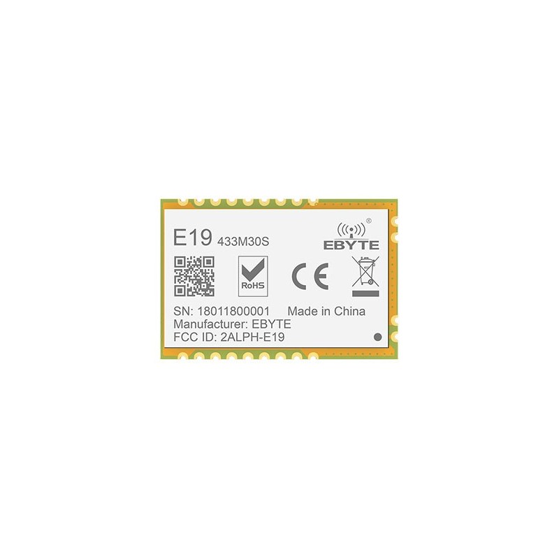
The E19-M30S 433MHz /868MHz /915MHz SPI +30dBm Enhanced Power LoRa Transceiver Module is based on original imported RFIC SX1278(433MHz) and SX1276(868MHz/915MHz) from SEMTECH, adopts LoRa spread spectrum technology.
The E19-M30S 433MHz /868MHz /915MHz SPI +30dBm Enhanced Power LoRa Transceiver Module is based on original imported RFIC SX1278(433MHz) and SX1276(868MHz/915MHz) from SEMTECH, adopts LoRa spread spectrum technology.
| RF Parameter | Value |
Remark |
| Working frequency |
410~931 MHz |
Default: 433MHz/868MHz/915MHz (32MHz oscillator) |
| Transmitting power | 30 dBm |
Max. Power (1W) |
| Receiving sensitivity | -148 dBm |
Air data rate: 0.3kbps |
| Air data rate | 0.018k~37.5kbps |
Default: 0.3kbps |
| Test distance | 10000m |
In open and clear air, with maximum power, 5dBi antenna gain, height of 2m, air data rate: 0.3kbps |
| Hardware Parameter | Value |
Remark |
|
Size |
25 * 37 mm |
|
|
Antenna type |
Stamp hole |
|
|
Communication interface |
SPI |
|
|
Package |
SMD |
|
| Electronic parameter | Min. | Typ. | Max. | Unit | Condition |
| Power supply |
3.3 | 5.0 | 5.5 | V | |
| Communication level | 1.8 | 3.3 | 3.6 | V | |
| Transmitting current |
570 | 630 | 690 | mA | 30dBm(1W) |
| Receiving current |
18 |
20 | 22 | mA | |
| Sleep current |
1.5 |
3.0 | 4.5 | μA | |
| Operating temperature |
-40 | 20 |
+85 | ℃ | |
| Operating humidity |
10 | 60 |
90 | % | |
| Storage temperature |
-40 | 20 |
+125 | ℃ |
| Pin No |
Pin item | Pin direction | Pin application |
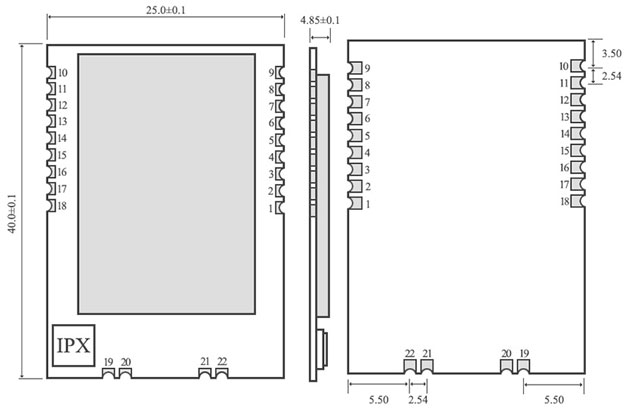
| 1 | GND |
- |
Ground electrode, connected to the power reference ground. |
| 2 | DIO5 | Input/Output |
Configurable IO port(Please find more on SX1276-7-8-9 Datasheet). |
| 3 | DIO4 | Input/Output |
Configurable IO port(Please find more on SX1276-7-8-9 Datasheet). |
| 4 | DIO3 | Input/Output |
Configurable IO port(Please find more on SX1276-7-8-9 Datasheet). |
| 5 | DIO2 | Input/Output |
Configurable IO port(Please find more on SX1276-7-8-9 Datasheet). |
| 6 | DIO1 | Input/Output |
Configurable IO port(Please find more on SX1276-7-8-9 Datasheet). |
| 7 | DIO0 | Input/Output |
Configurable IO port(Please find more on SX1276-7-8-9 Datasheet). |
| 8 | RST | Input |
Reset |
| 9 | GND | - |
Ground electrode, connected to the power reference ground. |
| 10 | GND | - |
Ground electrode, connected to the power reference ground. |
| 11 | VCC | - |
Power supply: 4.75~5.5V (Ceramic filter capacitoris advised to add) |
| 12 | SCK | Input |
SPI clock |
| 13 | MISO | Output |
SPI clock |
| 14 | MOSI | Input |
SPI clock |
| 15 | NSS | Input |
Chip select |
| 16 | TXEN | Input |
Radio frequency switch control, make sure the TXEN pinis in high level, RXEN pin is in low level when transmitting. |
| 17 | RXEN | Input |
Radio frequency switch control, make sure the TXEN pinis in high level, RXEN pin is in low level when transmitting. |
| 18 | GND | - |
Ground electrode, connected to the power reference ground |
| 19 | ANT | - |
Antenna |
| 20 | GND | - |
Ground electrode, connected to the power reference ground |
| 21 | GND | - |
Ground electrode, connected to the power reference ground |
| 22 | GND | - |
Ground electrode, connected to the power reference ground |
Reference: DWM14073001
Brand: Semtech
APC340 LoRa series rf module is built in RFIC sx1278 and sx1276 which can work on 433MHz,470MHz ,868MHz,915MHz 20dBm Ultra Long Range Transceiver Module with LoRa spread spectrum modulation.
Reference: DWM15123001
Brand: Semtech
HM-TRLR-S series are operating at 433MHz, 868MHz, 915MHz low cost, high performance transparent transceiver with LoRa/FSK/ GFSK/OOK modulation variety.It's mainly use for uav controller and drone data link.
Reference: DWM16092701
RFM98PW / RFM95PW which are Enhanced Power Long Range Transceiver Module.the available versions is RFM98PW 433MHz, and 868MHz,915MHz for RFM95PW.
Reference: DWM16112801
DWM-LoRa1276F30 is a 500W high power wireless transceiver module, which integrates SemtechRF transceiver chip SX1276. There are 868MHz and 915MHz for avaialble options.
Reference: DWM19070805
RAK7205 LoRa Tracker With Solar Panel built on RAK5205 integrated the Ublox Max 7Q module built on SX1276 LoRaWAN modem with low power micro-controller STM32L1.
Reference: DWM18103001
USD30/pcs MOQ100pcs The Lora/GPS Arduino Shield is with 433MHz /868MHz /915MHz Versions is a expension board of LoRa™/GPS for use with the arduino.This product is intended for those interested in developing LoRa™/GPS solutions.
Reference: DWM17092902
$8.5/pcs MOQ100pcs RFM98PW / RFM95PW which are Enhanced Power Long Range Transceiver Module.the available versions is RFM98PW 433MHz, and 868MHz,915MHz for RFM95PW.
Reference: DWM18110601
Brand: Semtech
RFM98W 433MHz,470MHz transceivers feature the LoRaTM long range modem It's from the HopeRF LoRa module.build by the semtech SX1278 chipset with the application for ARM meters.
Reference: DWM17120404
0.96 OLED Display ESP32 WIFI Bluetooth SX1278 433MHz Lora IOT Development Board for Arduino Smart Home.
Reference: DWM19022803
DWM-RAK2245 Pi HAT Raspberry Pi 3B Lora tracker start kit is a LoRaWAN gateway Module based on SX1301,Pre-install LoRa gateway OS.
Reference: DWM16092701
RFM98PW / RFM95PW which are Enhanced Power Long Range Transceiver Module.the available versions is RFM98PW 433MHz, and 868MHz,915MHz for RFM95PW.
Reference: ODL25030701
The nRFLR1262 module integrates the Nordic nRF52840 microcontroller and the Semtech SX1262 LoRa transceiver chip supports Bluetooth 5.3 and low-power Bluetooth and LoRaWAN 1.0.3 specification. It also supports the LoRa point-to-point (P2P) communication mode.
Reference: DWM16050805
Brand: Semtech
HM-TRLR-D series are operating at 433MHz, 868MHz, 915MHz low cost, high performance transparent transceiver with LoRa/FSK/ GFSK/OOK modulation variety.It's mainly use for uav controller and drone data link.
Reference: DWM18051402
Brand: Semtech
HPD14A SX1278 433MHz /470MHz LoRa Wireless transceiver module feature the LoRaTM long range modem It's from the HopeRF LoRa module.build by the semtech chipset with the application for ARM meters.
Reference: DWM16112802
DWM-LoRa1278F30 is a 500W high power wireless transceiver module, which integrates SemtechRF transceiver chip SX1278. There are 433MHz and 470MHz for avaialble options.
Reference: DWM19091701
DWM-RAK2245 SX1301 8 Channels Stamp Edition is a LoRaWAN gateway Module based on SX1301,Pre-install LoRa gateway OS.
Reference: DWM15123001
Brand: Semtech
HM-TRLR-S series are operating at 433MHz, 868MHz, 915MHz low cost, high performance transparent transceiver with LoRa/FSK/ GFSK/OOK modulation variety.It's mainly use for uav controller and drone data link.
Reference: DWM18110602
Brand: Semtech
RFM95W transceivers with 868 MHz and 915 MHz feature the LoRa TM long range rf module which core chipset are the semtech serice LoRa SX1276 chipset,usually build for the ARM application.
Reference: DWM20052801
The DWM-RAK7204 is an LPWAN node that serves as an environmental monitoring station. The high-precision sensors, can measure changes in temperature, humidity, gas pressure and provide an indoor air quality index.
Reference: DWM20060102
Brand: Semtech
DWM-RAK4200 Breakout Module is specifically designed to allow easy excess to the pins on the module in order to simplify development and testing.it's utilized is of an Xbee form factor.

The E19-M30S 433MHz /868MHz /915MHz SPI +30dBm Enhanced Power LoRa Transceiver Module is based on original imported RFIC SX1278(433MHz) and SX1276(868MHz/915MHz) from SEMTECH, adopts LoRa spread spectrum technology.