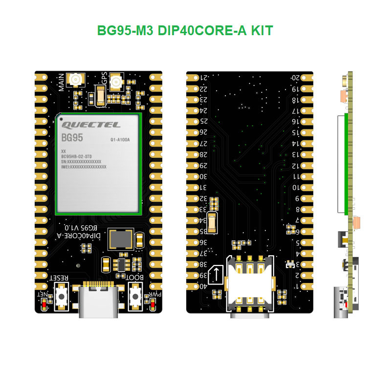
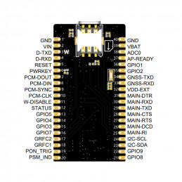
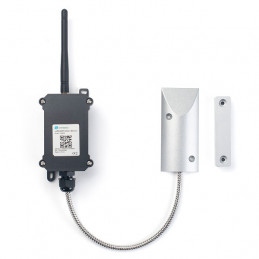
pin
assignment
of BG95
40PIN DTP
PCBA |
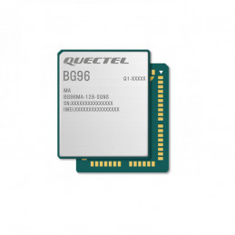
pin
assignment
of BG95
module |
Pin Name |
Description |
DC
Characteristics |
Comment |
| 1 |
|
GND |
Ground |
|
|
| 2 |
|
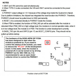
VIN |
Power supply for
the PCBA |
Vmax = 12 V
Vmin = 4.8 V
Vnorm = 5 V |
Cannot be used
simultaneously with
VBAT pins |
| 3 |
23 |
D-TXD |
Debug UART
transmit |
VOLmax = 0.45 V
VOHmin = 1.35 V |
1.8 V power domain.
If unused, keep this
pin open. |
| 4 |
22 |
D-RXD |
Debug UART
receive |
VILmin =-0.3 V
VILmax = 0.6 V
VIHmin = 1.2 V
VIHmax = 2.0 V |
1.8 V power domain.
If unused, keep this
pin open. |
| 5 |
17 |
RESET |
Reset the
module |
Vnorm = 1.5 V
VILmax = 0.45 V |
|
| 6 |
15 |
PWRKEY |
Turn on/off the
module |
Vnorm = 1.5 V
VILmax = 0.45 V |
PWRKEY should
never be pulled
down to GND
permanently |
| 7 |
7 |
PCM-DOUT |
PCM data output |
VOLmax = 0.45 V
VOHmin = 1.35 V |
1.8 V power domain.
If unused, keep this
pin open. |
| 8 |
6 |
PCM-DIN |
PCM data input |
VILmin =-0.3 V
VILmax = 0.6 V
VIHmin = 1.2 V
VIHmax = 2.0 V |
1.8 V power domain.
If unused, keep this
pin open. |
| 9 |
5 |
PCM-SYNC |
PCM data frame
sync |
VOLmax = 0.45 V
VOHmin = 1.35 V |
1.8 V power domain.
If unused, keep this
pin open. |
| 10 |
4 |
PCM-CLK |
PCM clock |
VOLmax = 0.45 V
VOHmin = 1.35 V |
1.8 V power domain.
If unused, keep this
pin open. |
| 11 |
18 |
W-DISABLE |
Airplane mode
control |
VILmin =-0.3 V
VILmax = 0.6
VVIHmin = 1.2 V
VIHmax = 2.0 V |
1.8 V power domain.
Pulled up by
default.When it is
in low
voltage level, the
module can enter
airplane mode.
If unused, keep this
pin open. |
| 12 |
20 |
STATUS |
Module
operation status
indication |
VOHmin = 1.35 V
VOLmax = 0.45 V |
1.8 V power domain.
If unused, keep this
pin open. |
| 13 |
66 |
GPI05 |
General-purpose
input/output |
VOLmax = 0.45 V
VOHmin = 1.35 V
VILmin =-0.3 V
VILmax = 0.6 V
VIHmin = 1.2 V
VIHmax = 2.0 V |
1.8 V power domain.
If unused, keep this
pin open. |
| 14 |
65 |
GPIO4 |
General-purpose
input/output |
VOLmax = 0.45 V
VOHmin = 1.35 V
VILmin =-0.3 V
VILmax = 0.6 V
VIHmin = 1.2 V
VIHmax = 2.0 V |
1.8 V power domain.
If unused, keep this
pin open. |
| 15 |
64 |
GPIO3 |
General-purpose
input/output |
VOLmax = 0.45 V
VOHmin = 1.35 V
VILmin =-0.3 V
VILmax = 0.6 V
VIHmin = 1.2 V
VIHmax = 2.0 V |
1.8 V power domain.
If unused, keep this
pin open. |
| 16 |
86 |
GPI07 |
General-purpose
input/output |
VOLmax = 0.45 V
VOHmin = 1.35 V
VILmin =-0.3 V
VILmax = 0.6 V
VIHmin = 1.2 V
VIHmax = 2.0 V |
1.8 V power domain.
If unused, keep this
pin open. |
| 17 |
84 |
GRFC2 |
Generic RF
controller |
VOLmax = 0.45 V
VOHmin = 1.35 V |
BOOT CONFIG.
Do not pull it up
before startup.
1.8 V power domain.
If unused, keep this
pin open. |
| 18 |
83 |
GRFC1 |
Generic RF
controller |
VOLmax = 0.45 V
VOHmin = 1.35 V |
1.8 V power domain.
If unused,keep this
pin open. |
| 19 |
96 |
PON TRIG |
Wake up the
module from
PSM |
|
1.8 V power domain.
Rising-edge
triggered.
Pulled-down by
default.
If unused, keep this
pin open. |
| 20 |
1 |
PSM-IND |
Power saving
mode indication |
VOHmin = 1.35V
VOLmax =0.45 V |
1.8 V power domain.
If unused, keep this
pin open. |
| 21 |
87 |
GPI08 |
General-purpose
input/output |
VOLmax = 0.45 V
VOHmin = 1.35 V
VILmin =-0.3 V
VILmax = 0.6 V
VIHmin = 1.2 V
VIHmax = 2.0 V |
1.8 V power domain.
If unused, keep this
pin open. |
| 22 |
88 |
GPIO9 |
General-purpose
input/output |
VOLmax = 0.45 V
VOHmin = 1.35 V
VILmin =-0.3 V
VILmax = 0.6 V
VIHmin = 1.2 V
VIHmax = 2.0 V |
1.8 V power domain.
If unused, keep this
pin open. |
| 23 |
41 |
I2C-SDA |
I2C serial data
(for external
codec) |
|
External pull-up
resistor is
required.
1.8 V only.
If unused, keep this
pin open. |
| 24 |
40 |
I2C-SCL |
I2C serial clock
(for external
codec) |
|
External pull-up
resistor is
required.
1.8 V only.
If unused, keep this
pin open. |
| 25 |
39 |
MAIN-RI |
Main UART ring
indication |
VOLmax = 0.45 V
VOHmin = 1.35 V |
1.8 V power domain.
If unused, keep this
pin open. |
| 26 |
38 |
MAIN-DCD |
Main UART data
carrier detect |
VOLmax = 0.45 V
VOHmin = 1.35 V |
1.8 V power domain.
If unused, keep this
pin open. |
| 27 |
37 |
MAIN-RTS |
Main UART
request to send |
VILmin =-0.3 V
VILmax = 0.6 V
VIHmin = 1.2 V
VIHmax = 2.0 V |
1.8 V power domain.
If unused, keep this
pin open. |
| 28 |
36 |
MAIN-CTS |
Main UART clear
to send |
VOLmax = 0.45 V
VOHmin = 1.35 V |
1.8 V power domain.
If unused, keep this
pin open. |
| 29 |
35 |
MAIN-TXD |
Main UART
transmit |
VOLmax = 0.45 V
VOHmin = 1.35 V |
1.8 V power domain.
If unused, keep this
pin open. |
| 30 |
34 |
MAIN-RXD |
Main UART
receive |
VILmin =-0.3 V
VILmax = 0.6 V
VIHmin = 1.2 V
VIHmax = 2.0 V |
1.8 V power domain.
If unused, keep this
pin open. |
| 31 |
30 |
MAIN-DTR |
Main UART data
terminal ready |
VILmin =-0.3 V
VILmax = 0.6 V
VIHmin = 1.2 V
VIHmax = 2.0 V |
1.8 V power domain.
If unused, keep this
pin open. |
| 32 |
29 |
VDD-EXT |
1.8V output
power supply for
external
circuits |
Vnorm = 1.8 V
I0max = 50 mA |
If unused, keep this
pin open |
| 33 |
28 |
GNSS-RXD |
GNSS UART
receive |
VILmin =-0.3 V
VILmax = 0.6 V
VIHmin = 1.2 V
VIHmax = 2.0 V |
1.8 V power domain.
If unused, keep this
pin open. |
| 34 |
27 |
GNSS-TXD |
GNSS UART
transmit |
VOLmax = 0.45 V
VOHmin = 1.35 V |
BOOT CONFIG.
Do not pull it up
before startup.
1.8 V power domain.
If unused, keep this
pin open. |
| 35 |
26 |
GPIO2 |
General-purpose
input/output |
VOLmax = 0.45 V
VOHmin = 1.35 V
VILmin =-0.3 V
VILmax = 0.6 V
VIHmin = 1.2 V
VIHmax = 2.0 V |
1.8 V power domain.
If unused, keep this
pin open. |
| 36 |
25 |
GPI01 |
General-purpose
input/output |
VOLmax = 0.45 V
VOHmin = 1.35 V
VILmin =-0.3 V
VILmax = 0.6 V
VIHmin = 1.2 V
VIHmax = 2.0 V |
1.8 V power domain.
If unused, keep this
pin open. |
| 37 |
19 |
AP-READY |
Application
processor sleep
state detection |
VILmin =-0.3 V
VILmax = 0.6 V
VIHmin = 1.2 V
VIHmax = 2.0 V |
1.8 V power domain.
If unused, keep this
pin open. |
| 38 |
24 |
ADCO |
General-purpose
ADC interface |
Voltage range:
0.1-1.8 V |
If unused, keep
these pins open. |
| 39 |
|
VBAT |
Power supply for
the module |
Vmax = 4.3 V
Vmin = 3.3 V
Vnorm = 3.8 V |
Cannot be used
simultaneously with
VIN pins |
| 40 |
|
GND |
Ground |
|
|