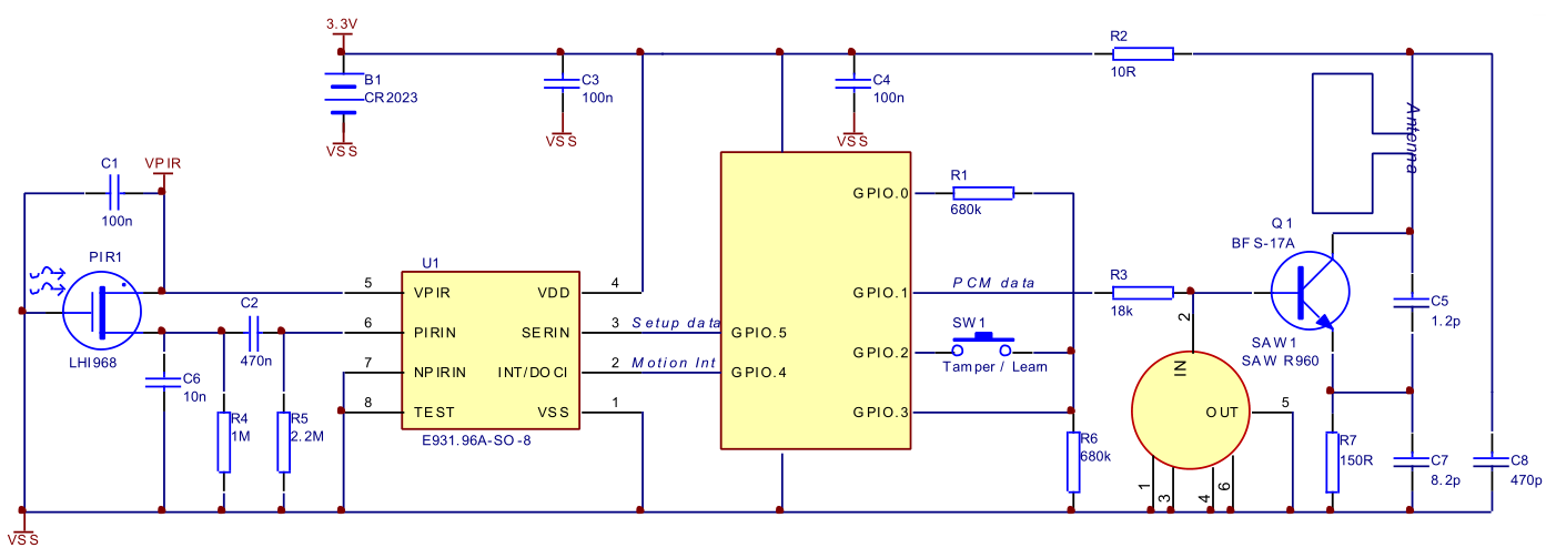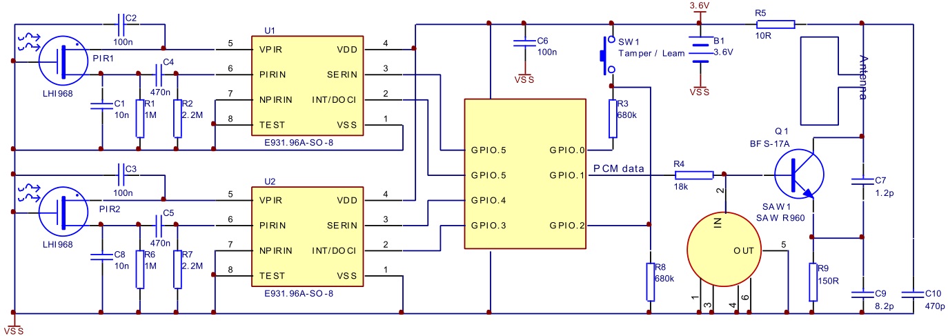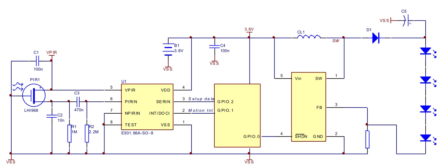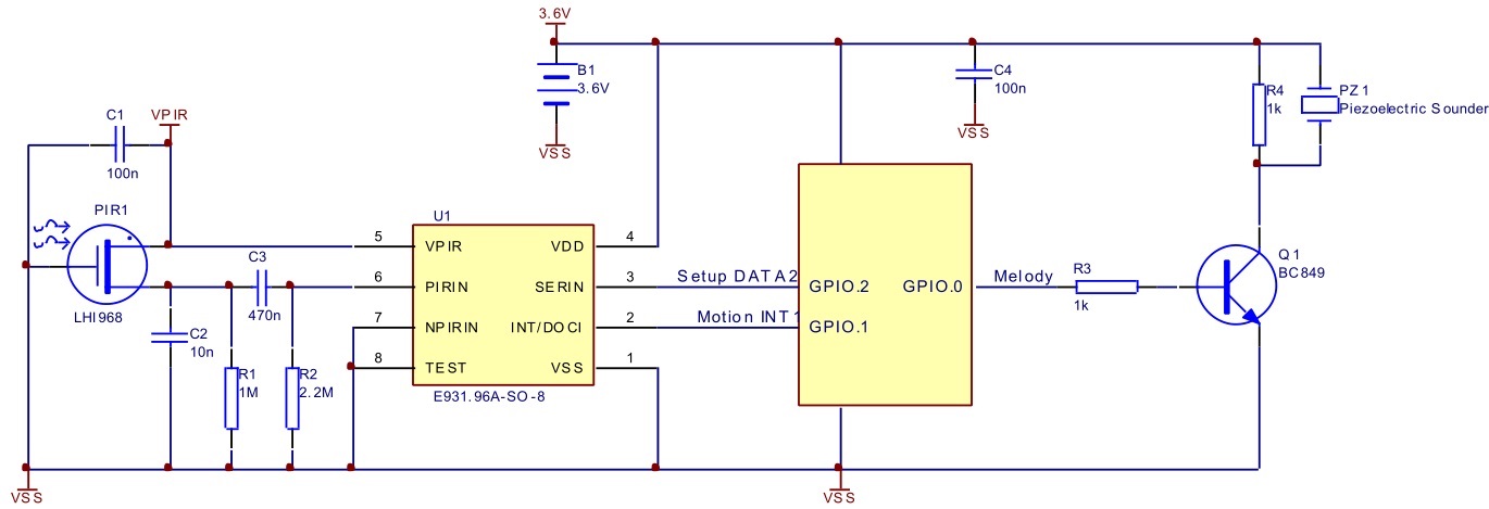
Affected Devices and Sensors
E931.96 Ultra-Low Power PIR Controller
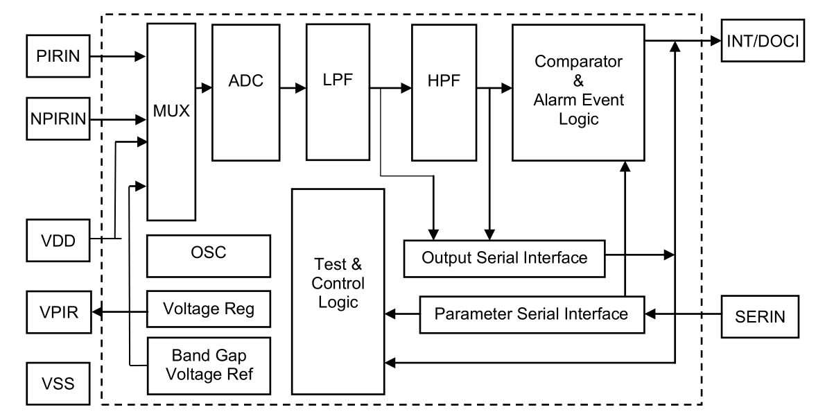
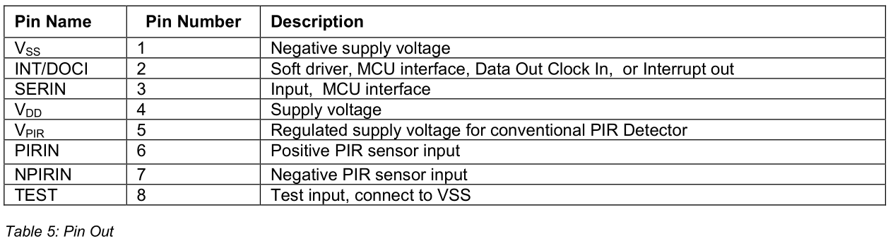
Interfaces
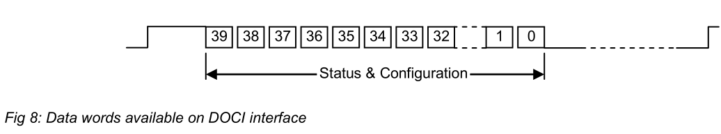
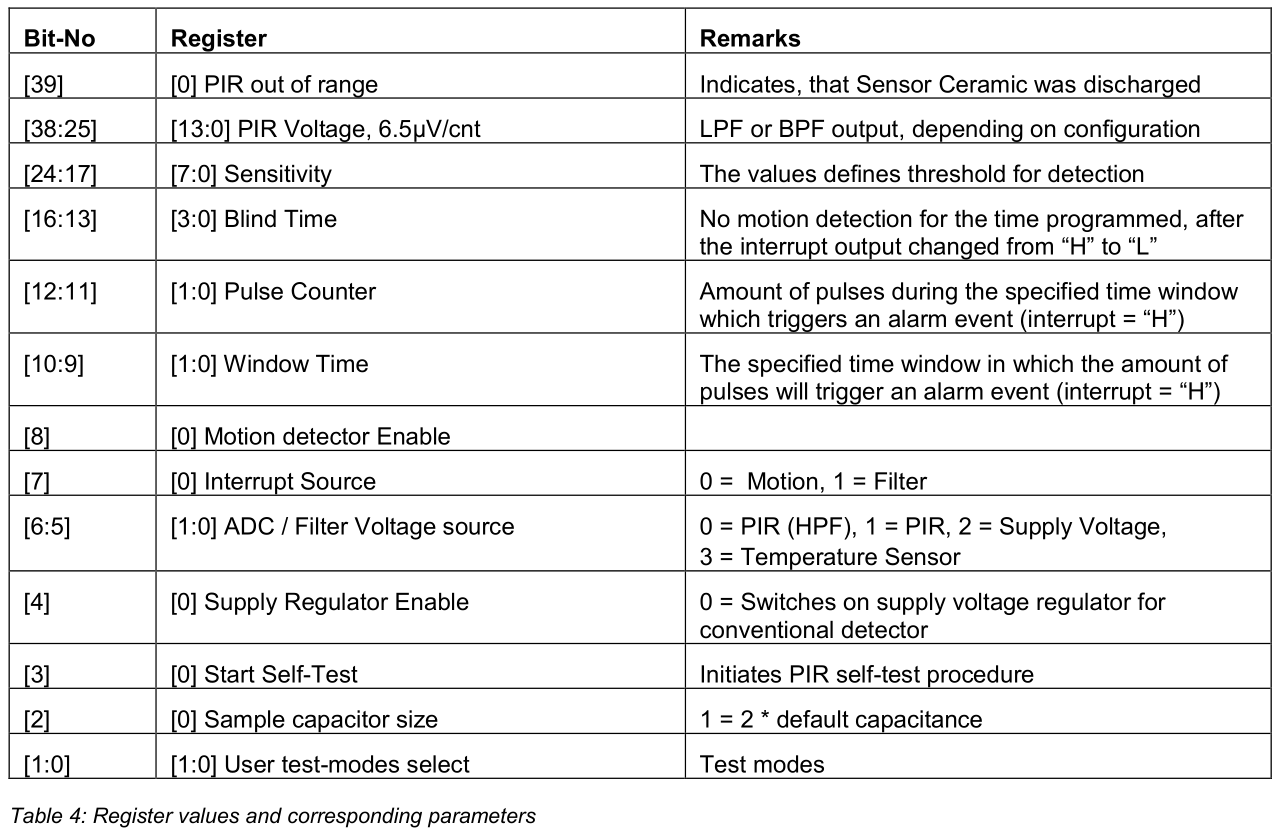
The E931.96 accepts data from the MCU on the SERIN input pin. Measurement data is clocked out and motion interrupts are flagged on the INT/DOCI pin of the device.A zero to one transition on the INT output indicates detected motion. The interrupt pin will stay at one until it is cleared by the MCU.The MCU can read the ADC voltages (14 bits) and the configuration data (25bits) through the DOCI output of the E931.96.
Setting up the device (SERIN)
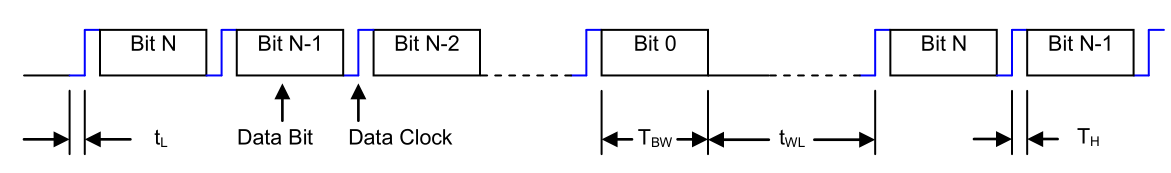
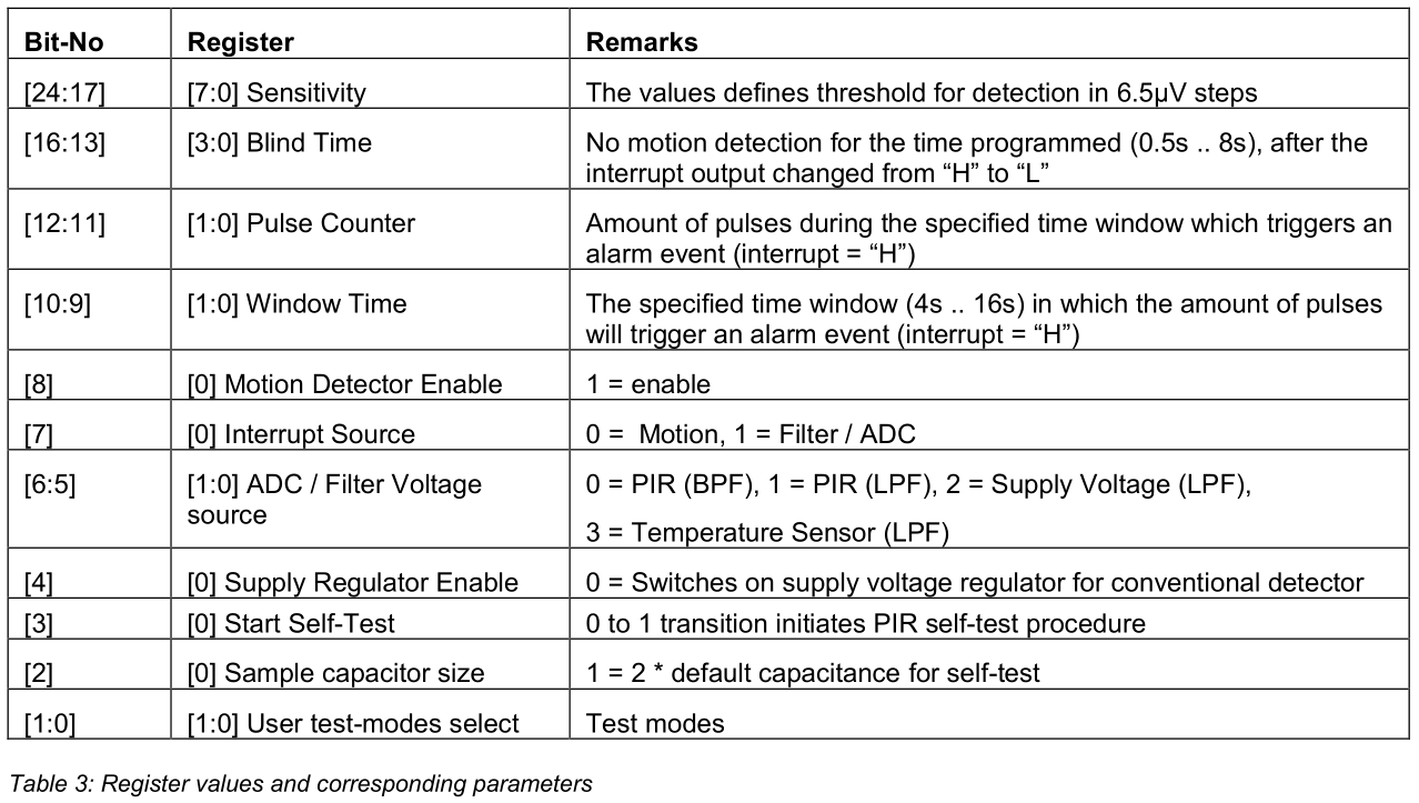
After power up the E931.96 need to be programmed with a configuration that sets up the device with operational parameters and puts the device in the correct operational mode. The device is programmed with a 25-bit bit stream on the SERIN input. The SERIN input is held low when the interface is not used, it also provides for minimum interference to the sensor. The microcontroller generates a low to high transition on the SERIN input, this is a clock pulse, and subsequently applies a data bit value, either a one or a zero. This process is repeated 25 times until all the data bits are clocked into the E931.96. The low to high transition or clock pulse can be very short, typically 1 instruction cycle of the microcontroller, but the data bit value must be applied for at least 2 system clocks (2/FCLK), of the E931.96. Whenever the data transfer is interrupted for more than 16 system clocks (16/FCLK), the last data received is latched into the configuration registers. Should the transfer of data be interrupted for more than 15 system clocks, the writing procedure needs to be restarted.Table 3 in the datasheet shows the sequence of bits and the meaning of the register values. Configuration data is clocked into the device starting at bit 24 down to bit 0. A typical code example would look as follows:
void write_to_E93196(long long setup_data) // setup_data holds the device configuration
{
char i;
long long mask;
mask=0x01000000; // Bitmask is at bit 25
for(i=0;i<25;i++)
{
serin_clock(); // Generates zero to one clock pulse on SERIN pin
if((setup_data&mask)>0) // Decide if it is a one or a zero data bit
output_high(SERIN);
else
output_low(SERIN);
delay_us(72); // More than 62us, ensure it is more than 2/FCLK
mask>>=1; // Shift mask to the next bit
}
output_low(SERIN);
delay_ms(1); // Wait for data to be latched, time must be more than 16/FCLK
}
Reading
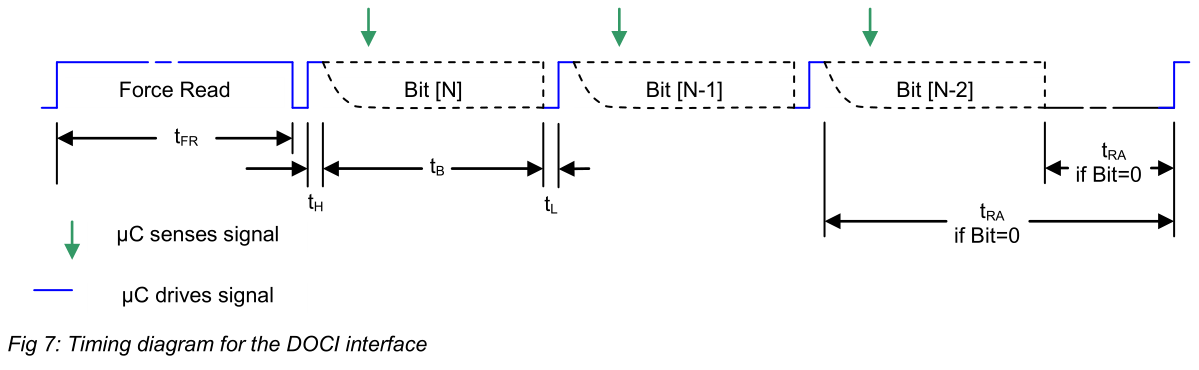
The DOCI pin is used to transfer data from the device to the MCU. The MCU drives a clock signal and the E931.96 provides the data bit. The MCU initiates reading of the status and configuration data by forcing a high level for the duration of more than 2 device clock cycles (>3/FCLK) on the DOCI pin (tFR in the datasheet).
A clock pulse is generated by a low to high transition on the DOCI pin. Subsequently the MCU samples data bit value driven by the E931.96. This process is repeated 15 times to read the ADC value and a further 25 times until all the data bits are clocked out of the E931.96. The sampling speed is influenced by the capacitance on the DOCI line due to the PCB layout and the MCU load. The DOIC pin does not have a strong driver so that it can be overdriven for the clock pulses. When readout is completed, the MCU must drive the DOCI pin to zero, and subsequently switch to tri-state in order to receive a new interrupt. The source for the ADC input can be selected between PIR input, supply voltage input and temperature. Reading can be terminated at any time by forcing the DOCI line to zero for at least 4 system clock cycles.The interrupt source for the DOCI/INT output can be selected between reading of the ADC values or for motion detection. If the ADC interrupt is selected, an interrupt is produced every 512 system clocks that signals that an ADC value is available to be clocked out. It is possible to read ADC values without making use of the interrupts generated by the E931.96.For interrupts as a result of motion, the motion detection bit and the interrupt source bit need to be set.No interrupt will be generated while the microcontroller accesses the interface.Below is an example of reading the ADC value as well as the configuration data from the device.
void readback_all_from_E93196(void)
{
int n;
long long kk;
#use fast_io(A) // This tells the compiler that I will take care of the direction settings of the port
force_doci_high(); // force read, hold DOCI high at least 3 clocks of IC
//clock out bits [39:25] for the ADC value and the out of range bit
for(n=0;n<(14+1);n++)
{
doci_clock();
adc<<=1; // This instruction is my sample delay
if(input(DOCI_PIN)==1)
adc++;
}
//Next read the setup bits [24:0]
setup_back=0;
for(n=0;n<25;n++)
{
doci_clock();
kk<<=1; // This instruction is my sample delay
if(input(DOCI_PIN)==1)
setup_back++;
} clear_DOCI_interrupt();
#use standard_io(A)
}
Helper functions
In the examples above we made use of small functions that is shown below. The syntax of these functions may be different to suit the particular compiler that is used. The DOCI output is clocked by the device as fast as possible; the direction handling is also taken care of.
void doci_clock(void)
{
#use fast_io(A)
output_low(DOCI_PIN); // Clear DOCI pin
doci_dir&=~DOCI_PIN_DIR; // Clear direction bit
set_tris_a(doci_dir); // DOCI pin output
delay_cycles(5); // Wait a bit
output_high(DOCI_PIN); // Set DOCI pin
doci_dir|=DOCI_PIN_DIR; // Set direction bit
set_tris_a(doci_dir); // DOCI pin input
delay_cycles(5); // Wait a bit
}
After an interrupt was generated by the device, it is cleared by the MCU by driving the DOIC pin low and releasing it, so that the device can drive again when an interrupt occurs.
void clear_DOCI_interrupt(void)
{
//Release the DOCI Line leave in zero state
#use fast_io(A) // Prevent compiler from handling the direction control
output_low(DOCI_PIN); // Clear DOCI pin
doci_dir&=~DOCI_PIN_DIR; // Clear direction bit
set_tris_a(doci_dir); // DOCI pin output
delay_cycles(175); // Time depends on track capacitance on the PCB
doci_dir|=DOCI_PIN_DIR; // Set direction bit
set_tris_a(doci_dir); // DOCI pin input
#use standard_io(A)
}
A read request from the MCU to the E931.96 is indicated by forcing DOCI to high level for 3 device clocks (3/FCLK) of the E931.96
void force_doci_high(void)
{
// force read, at least 3 clocks of IC
#use fast_io(A) // Prevent compiler from handling the direction control
output_high(DOCI_PIN); // Set DOCI pin
doci_dir&=~DOCI_PIN_DIR; // Clear direction bit
set_tris_a(doci_dir); // DOCI pin output
delay_us(120);
#use standard_io(A)
}
The function below generates the clock signal on the SERIN input of the device. The clock delay can be as short as one cycle on the MCU.
void serin_clock(void)
{
output_low(SERIN); // Clear SERIN pin
delay_us(1);
output_high(SERIN); // Set SERIN pin
delay_us(1);
}
2C9EA1IK3B.png)